Are you wondering how that small silicon disc, the wafer, can have such a significant impact on the power of your solar panel? It’s perfectly normal, because without it, there’s no green electricity! Let’s explore together why this component is so important and how it influences the performance, cost, and even the future of solar energy. Get ready to discover the fascinating world of wafers!
Key Takeaways
- The wafer is the heart of your solar cell: it converts sunlight into electricity. Its purity and well-processed surface are crucial for it to work effectively.
- The thickness and size of the wafer are a bit like choosing the right size for clothing: it needs to be adapted. Doping is what allows electrical current to flow easily.
- The price of the wafer plays a big part in the final cost of your panel. A balance needs to be struck between a quality product and an affordable price.
- Manufacturers never stop innovating! They are developing ways to make cheaper and more efficient wafers, using new materials or more refined techniques.
- For your panel to last a long time, the wafer needs to be well protected. The quality of the material and how it’s integrated into the panel are important for its longevity.
The Importance of the Wafer for Solar Performance
Hello! Let’s talk a bit about the heart of your solar panels: the wafer. It’s this thin slice of silicon that does all the work of converting light into electricity. Without it, there’s no solar magic! It’s truly the foundation upon which the entire performance of your installation rests.
How the Wafer Converts Light into Electricity
Imagine the wafer as a very special stage. When the sun’s rays, which are actually photons, arrive and strike this silicon stage, they give a boost to the electrons. Once these electrons receive this energy, they start to move. This movement of electrons is what constitutes electric current! This is the photovoltaic effect, and the wafer is its main actor. It’s a bit like a switch that turns on when there’s light, but instead of lighting up a bulb, it creates electricity.
The Influence of Silicon Purity on Efficiency
The quality of the silicon used to make the wafer is extremely important. The purer the silicon, the better. Why? Because small impurities in the silicon can act as obstacles for the electrons. They essentially trap them, preventing them from moving freely. Fewer electrons moving means less electricity produced. Manufacturers therefore do a tremendous job of obtaining the purest possible silicon. It’s a bit like wanting a very smooth road so cars can drive fast, without bumps or potholes.
The purity of silicon is a determining factor: high-purity silicon ensures better conversion of light into electricity.
Optimising the Wafer Surface to Capture More Light
For your solar panel to be as efficient as possible, the wafer needs to be able to capture a maximum amount of light. There are several tricks for this. For example, we can play with the surface texture so that it reflects less light and absorbs more. We can also consider how the electrical contacts are placed. They are often in the form of a very fine grid on the top so as not to cover too much surface, and they cover the entire underside. The goal is not to miss a single ray of sunshine! The solar wafer market is growing rapidly, which clearly shows their importance in the solar energy sector.
Here are some key points for optimising light capture:
- Surface Treatment: Creating micro-structures to trap light.
- Anti-reflective Coatings: Applying special layers to reduce reflection.
- Contact Arrangement: Minimising shading caused by metal grids.
Essentially, every detail counts for your wafer to transform as much light as possible into usable electricity. It’s a bit like a puzzle where each piece must be perfectly fitted for the final image to be the best it can be.
Key Characteristics That Define a Good Wafer
So, what makes a wafer truly good for your solar panel? It’s not just a simple silicon disc, far from it! Several technical aspects play a crucial role in ensuring your installation captures maximum sunlight and converts it into electricity.
Wafer Thickness: A Compromise Between Strength and Absorption
You might be wondering why wafer thickness is so important. Well, it’s a bit of a balancing act. A thicker wafer will be more robust, less likely to break during manufacturing or when you handle the panel. But be careful, a wafer that’s too thick might not absorb light as well. The right balance needs to be found so it’s strong without losing efficiency. We often talk about a few hundred micrometres, which is really thin when you think about it!
Wafer Size and its Impact on Panel Power
Size matters, especially in the world of solar! The larger your wafer, the more surface area there is to capture the sun’s rays. Makes sense, right? A larger wafer can therefore potentially produce more electricity. This is why you see more and more panels with increasingly larger solar cells. It also helps reduce manufacturing costs per watt produced, which is good news for your wallet. The wafer market is actually growing rapidly, a sign that everyone wants more solar power [f06c].
The Crucial Role of Doping for Electrical Properties
Doping is a bit like the magic that makes silicon conductive. By adding small amounts of other elements to pure silicon, its electrical properties are modified. This is what allows the creation of the famous “p-n junction” in the solar cell, which will enable the separation of electrical charges generated by light. Without carefully controlled doping, your wafer would just be a simple piece of silicon, incapable of conducting current. It’s truly a technical step that requires great precision.
The wafer is the foundation of everything in a solar cell. Its purity, thickness, size, and how it’s chemically treated (doping) directly determine its ability to convert light into electricity. It’s a bit like choosing the right ingredients for a cake: if the base isn’t good, the result won’t be up to par.
Here are some points to remember about the characteristics of a good wafer:
- Silicon Purity: The purer it is, the better for light conversion.
- Absence of Crystal Defects: Imperfections can reduce efficiency.
- Uniform Thickness: For good current distribution.
- Size and Shape: Influence the total panel power and production costs.
- Doping Quality: Essential for creating the necessary electric field.
How the Wafer Influences the Cost of Solar Panels
Hello! Let’s talk a bit about what goes into the price of your solar panels, and more specifically, the role of the wafer. You see, the wafer is essentially the heart of the solar cell. And as with many things, the quality and how it’s manufactured have a direct impact on the final price.
Wafer Prices: A Determining Factor in the Budget
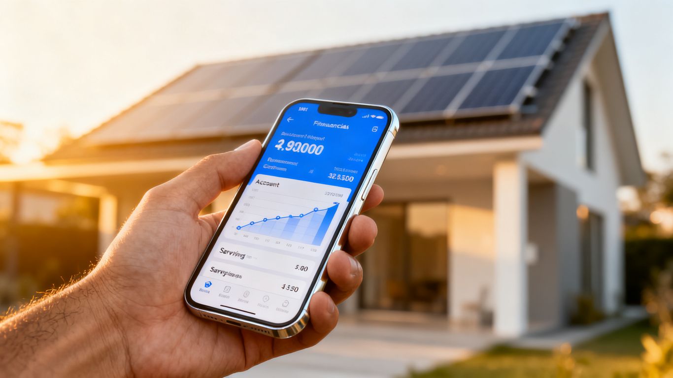
It’s important to know that the wafer represents a significant portion of the total cost of a solar panel. It’s a bit like the cost of flour for a baker; without it, there’s no bread! Several factors influence the price of a wafer: the purity of the silicon used, its size, and of course, the technologies employed to manufacture it. Manufacturers therefore have to find a balance to keep their panels competitive in the market. The cost of the wafer is therefore a key element in the overall budget of your solar installation.
Finding the Balance Between Wafer Quality and Competitiveness
This is where it gets interesting. One might think: “Why not use cheaper wafers?” Well, it’s tempting, but you have to be careful. For example, using thinner wafers can reduce costs, but they become more fragile. Or, using less pure silicon can also lower the price, but this directly affects the panel’s performance. Less electricity produced means less profitability in the long run. Therefore, you need to carefully consider what you want: a lower initial purchase price, or better energy production over time? It’s a bit like choosing between a cheap used car that needs repairs and a slightly more expensive but more reliable car. The choice depends on your priorities, and for solar, it directly impacts the cost per peak watt of your installation.
Strategies to Reduce Costs Without Sacrificing Performance
Fortunately, manufacturers aren’t standing still. They are constantly looking for ways to improve things. For example, they are working on techniques to make wafers larger, which allows for the production of more powerful cells. They are also refining cutting methods to minimise silicon waste. Factory automation also helps reduce production costs while improving quality. And then there’s research into new materials, like perovskite, which could one day change the game and make solar even more accessible. It’s a bit like optimising a recipe: you aim to use the best ingredients, but also to be more efficient in preparation to achieve a delicious and affordable dish.
It’s important to remember that the wafer is only one part of the panel. Its quality must be consistent with the other components: the glass, the encapsulant, the frame. Everything must work together for the panel to last a long time and produce well.
Here are some avenues for improving production and reducing costs:
- Reducing Wafer Thickness: Less raw material used, therefore cheaper.
- Improving Texturing: So the wafer captures light even better.
- Automating Processes: For faster manufacturing and fewer errors.
- Research into New Materials: Such as perovskite, which promises interesting advancements.
Technological Advancements Shaping Tomorrow’s Wafers
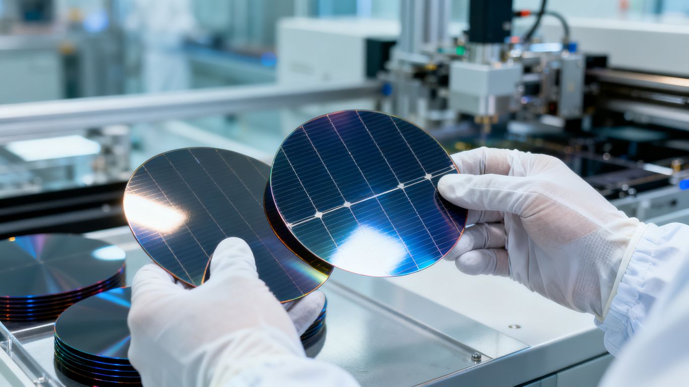
Hello! Let’s talk a bit about what’s happening in the world of solar wafers. Just because silicon has been around for a long time doesn’t mean we’ve stopped looking for improvements, far from it! Researchers and engineers are working tirelessly to make these small discs even more efficient and affordable.
Innovations in Wafer Manufacturing Processes
You know, making a wafer is a bit like high-end cooking: you need quality ingredients and a super-controlled environment. We’re talking about purifying silicon to an incredible degree, then slicing it into thin discs like paper. Techniques are constantly evolving to make these steps more efficient and less costly. For example, we’re looking to reduce the amount of silicon used while maintaining good strength. The idea is to be able to produce more wafers, faster, and with less waste. It’s a bit like optimising a recipe to make it better and quicker to prepare. We’re also seeing methods to *stretch* molten silicon, which can change how crystals form and, ultimately, improve wafer quality. It’s a bit like trying new cooking techniques to get a better result.
The Emergence of New Generations of Wafers
Monocrystalline silicon is currently the champion, but other avenues are being explored. We’re seeing wafers with slightly different structures, like heterojunction (HJT), which allow for even more light capture and reduced energy loss. It’s as if a special layer is added to better catch the sun’s rays. And then there’s research into completely new materials, like graphene or other compounds. These materials could offer even better electrical properties than silicon, although we are still in the early stages for large-scale solar applications. The goal is clear: push the boundaries of efficiency.
Evolutionary Prospects for More Efficient Wafers
So, what can we expect for the future? Well, wafers will likely become even larger. This allows for the production of more powerful solar panels, which is good news for us. We will also continue to look for cheaper and more efficient materials than silicon, to make solar energy even more accessible. And then there’s the idea of integrating wafers into smarter systems, capable of managing energy more finely. Imagine panels that not only produce electricity but also help optimise its consumption. It’s a bit like moving from a simple light bulb to a smart lighting system. The European industry, for example, is working to strengthen its production capabilities to avoid dependence on other regions, with ambitious goals for silicon wafer production.
The manufacturing of solar wafers is a constantly evolving field. Innovations aim to improve efficiency, reduce costs, and explore new materials, while maintaining high quality standards. These advancements are essential to make solar energy increasingly competitive and accessible.
Ensuring the Longevity and Reliability of Solar Wafers
Factors Affecting the Lifespan of a Wafer
You’re probably wondering how long these little silicon marvels will last. Well, several things come into play. First, there are the weather conditions: the sun beats down, it rains, it freezes, it thaws… all of this causes wear. Humidity is a sworn enemy of the wafer, as are significant temperature fluctuations. The quality of the silicon itself is extremely important. A pure wafer, carefully manufactured, will be more durable over time. And then, beware of shocks or vibrations, which can create invisible micro-cracks that, in the long run, reduce performance. It’s a bit like with an old car; the better maintained and higher quality it is from the start, the longer it runs.
Wafer Protection Measures in Solar Panels
For your solar panels to keep going for years, manufacturers go all out to protect the wafers. It’s a bit like putting a helmet and protective gear on an athlete.
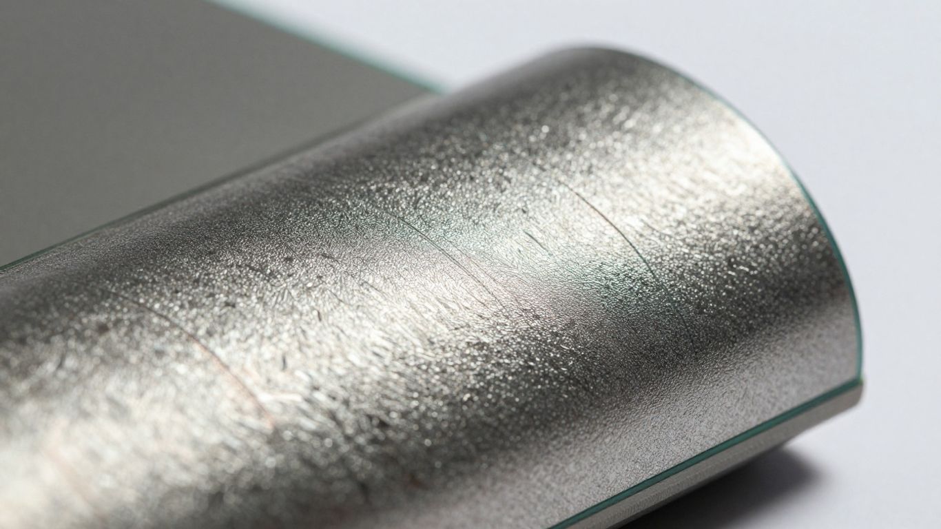
- Encapsulation: The wafer is sandwiched between protective layers, often EVA (ethylene-vinyl acetate). This protects it from moisture and dust.
- Tempered Glass: The front face is made of robust glass, resistant to impacts (like hail) and weathering.
- Frame: Often made of aluminium, it provides good rigidity to the assembly and protects the fragile edges of the wafer.
These protections are in place to minimise degradation. Even though a slight decrease in performance is normal over time, these measures make a real difference to the lifespan of your panels. By the way, to get an idea of manufacturers who do this well, you can look at the big names in the photovoltaic market.
The Importance of Component Compatibility in the Panel
It’s not enough to have a good wafer and good protection. Everyone needs to play on the same team! The glass, the encapsulating film, the frame, and of course the wafer, everything must be compatible. If one element isn’t suitable, it can create problems and reduce overall performance, or even the panel’s lifespan. It’s a bit like assembling a puzzle: all the pieces must fit together perfectly for the image to be beautiful and last over time. Thinking about compatibility also means thinking about durability and long-term performance, much like when choosing materials that comply with environmental standards, for example to limit harmful substances.
Exploring New Horizons with Flexible Wafers and Innovative Materials
Hello! We’re now going to talk about what happens when we step a bit outside the box with wafers. You know, we’ve talked about silicon, purity, all that. But the world of solar is constantly changing, and there are some really cool things in the pipeline.
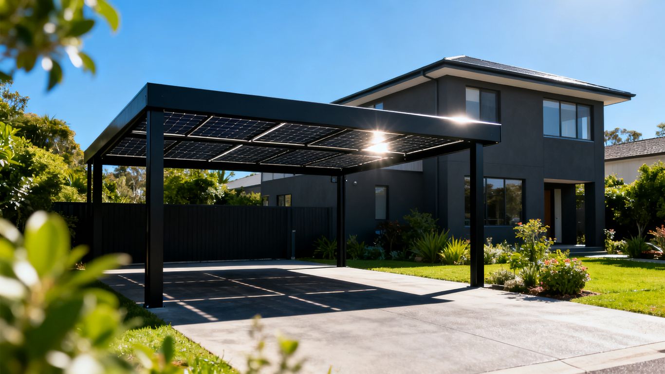
Advantages of Flexible Wafers for Various Applications
Just imagine: solar panels that aren’t rigid like boards. That’s the idea behind flexible wafers. They are super practical because they can adapt to many shapes. Think about building facades that aren’t flat, or even your car roof. This opens up possibilities for putting solar power almost anywhere, even on objects we wouldn’t have imagined. It’s a way to make solar energy more discreet and more integrated into our daily lives. Thin-film technology is also an interesting avenue for making all of this possible.
Research into Alternative Materials like Perovskite
Silicon is good, but it’s not the only player on the field. Researchers are exploring many new materials. One that’s generating a lot of buzz is perovskite. It’s a bit like a promising newcomer in the world of solar cells. Scientists are working hard to improve its efficiency and stability. The idea is to see if we can do even better than silicon, perhaps even at a lower cost. It’s an area with a lot of experimentation, and we’re seeing results that are encouraging. For example, studies show that perovskite-based solar cells could well be a game-changer.
Continuous Efficiency Improvement Through New Technologies
Ultimately, all of this revolves around a simple idea: making solar panels more efficient. Whether it’s with larger wafers, different materials, or more refined manufacturing techniques, the goal is always the same. We aim to capture more sunlight and convert it into electricity more efficiently. It’s a bit like a race for innovation. Progress is constant, and that’s what makes the solar field so dynamic. We can expect to see increasingly efficient solar panels adapted for even more varied uses in the coming years.
Want to discover the future of energy? Flexible wafers and cutting-edge materials are opening up incredible doors for new and exciting applications. Imagine lighter, more adaptable, and more efficient technologies! Curious to learn more about these game-changing advancements? Visit our website to explore how these innovations can transform your project.
So, What’s the Takeaway?
There you have it, you now know how incredibly important the wafer is for your solar panels. It’s truly the foundation of everything, the thing that allows your roof to produce clean electricity. We’ve seen that its purity, thickness, and even its surface all make a difference in capturing sunlight and converting it into current. And don’t forget that all of this also affects the price of the panels. It’s a bit of a puzzle for manufacturers to find the right balance between quality and cost. But with all the research and new ideas emerging, it promises even more efficient and affordable panels for everyone. So, the next time you look at a solar panel, think about that little piece of silicon that makes all the magic happen!
Frequently Asked Questions
What exactly is a wafer and why is it so important for solar power?
Imagine the wafer as the heart of your solar panel. It’s a thin slice, often made of super-pure silicon, that has the superpower to transform sunlight into electricity. Without a good wafer, your panel won’t produce much energy.
Does the purity of silicon really change the amount of electricity produced?
Absolutely! The purer the silicon, the better. Small impurities in silicon act like brakes for the electrons that create electricity. So, a very pure wafer allows for the manufacture of more efficient panels that produce more energy.
Why do wafers have different thicknesses and sizes?
It’s a bit like choosing the right shoe size! A thicker wafer is more robust but might not capture light as well. A larger wafer allows for a more powerful panel, but it costs more. Manufacturers look for the best compromise for each type of panel.
How does the wafer influence the final price of a solar panel?
The wafer is often the most expensive component of the panel. Its manufacturing requires a lot of technology and quality materials. Therefore, a high-quality wafer costs more, which drives up the panel’s price. It’s a bit of a challenge to have high-performance panels without them costing a fortune.
What are the latest innovations to make wafers even better?
Researchers are working tirelessly! They are inventing new ways to manufacture wafers, sometimes thinner, sometimes with special structures to capture even more light. They are also exploring new materials, like perovskite, which could make future panels even more efficient and cheaper.
How long will a solar panel function thanks to its wafer?
A good wafer, well protected within its panel, can last a very long time, often over 25 years! Its lifespan depends on the quality of the silicon, how it was manufactured, and its protection against rain, wind, and temperature changes. It’s truly built to last!